In the fast-paced world of microelectronics, the foundation for creating intricate electronic components lies in photolithography. This revolutionary process plays a pivotal role in manufacturing integrated circuits and microchips that power our modern devices. Photolithography is a vital source of knowledge in the realm of microelectronics, enabling the precise fabrication of intricate patterns on semiconductor wafers. In this article, we will delve into the fascinating world of photolithography, exploring its principles, applications, and significance in shaping the landscape of modern technology.
1. Understanding Photolithography
1.1 What is Photolithography?
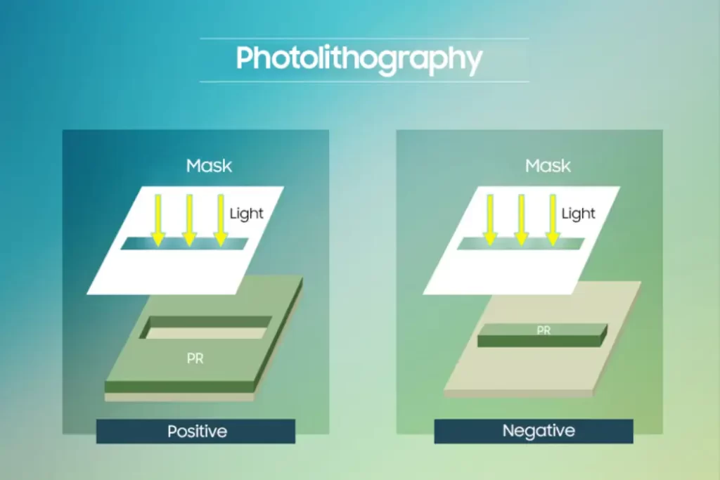
Photolithography is a fundamental process used in the semiconductor industry to create intricate patterns on silicon wafers. It involves projecting a precise pattern from a photomask onto a photosensitive material called photoresist. This pattern transfer is a crucial step in the manufacturing of integrated circuits and microchips.
1.2 Historical Background
The roots of photolithography can be traced back to the late 19th century when the first photoresist was discovered. However, its true potential was unlocked in the mid-20th century, leading to significant advancements in microelectronics.
1.3 Evolution of Photolithography
Over the years, photolithography has undergone remarkable transformations, driven by the relentless pursuit of higher resolutions and smaller feature sizes. From simple contact printing to advanced stepper and scanner systems, each evolution has paved the way for the modern era of microelectronics.

2. Key Components of Photolithography
2.1 Photoresist
Photoresist is a light-sensitive material that undergoes chemical changes when exposed to light. It serves as a crucial medium to transfer patterns onto the silicon wafer during the photolithography process.
2.2 Photomask
A photomask is a transparent plate with a specific pattern used to define the desired circuit layout. It acts as a stencil through which light is passed to create the pattern on the photoresist.
2.3 Exposure System
The exposure system consists of a light source, projection optics, and a mechanism to align the photomask and wafer accurately. It is responsible for precisely transferring the pattern onto the photoresist.
2.4 Developing and Etching
After exposure, the photoresist is developed, either removing the exposed or unexposed regions. This step creates the pattern that will guide subsequent etching processes to define the circuitry.
3. The Photolithography Process
Step 1: Cleaning and Preparation
Before the photolithography process begins, the silicon wafer is thoroughly cleaned to remove any impurities or contaminants that could interfere with the pattern transfer.
Step 2: Applying Photoresist
A thin layer of photoresist is spin-coated onto the wafer’s surface. The photoresist is then pre-baked to ensure uniformity and adhesion.
Step 3: Exposing the Photomask
The photomask, containing the desired pattern, is aligned with the wafer and exposed to light. The light passing through the transparent areas of the mask interacts with the photoresist, inducing a chemical change.
Step 4: Developing and Etching
The exposed photoresist is developed, creating a pattern on the wafer surface. This pattern is used as a mask during subsequent etching processes to transfer the pattern into the underlying substrate.
4. Steppers and Scanners: Advancements in Photolithography
4.1 Steppers
Steppers are photolithography tools that use a step-and-repeat process to expose a pattern multiple times on the wafer. They have been instrumental in achieving high throughput and precision.
4.2 Scanners
Scanners, on the other hand, use a continuous motion to expose the wafer, eliminating the need for step-and-repeat. They offer improved resolution and are widely used for advanced manufacturing.
4.3 Resolution Enhancement Techniques
To overcome the limitations of optical diffraction, resolution enhancement techniques like optical proximity correction (OPC) and phase-shift masks (PSM) have been introduced to enhance pattern fidelity.
5. Applications of Photolithography
5.1 Semiconductor Industry
The semiconductor industry heavily relies on photolithography to fabricate intricate semiconductor devices, such as microprocessors, memory chips, and sensors.
5.2 Display Technology
Photolithography is crucial for producing high-resolution displays found in smartphones, TVs, and computer monitors.
5.3 MEMS and NEMS Devices
Micro-electromechanical systems (MEMS) and nano-electromechanical systems (NEMS) devices also benefit from photolithography in their manufacturing processes.

6. Challenges and Future Trends
6.1 Pushing the Limits of Resolution
As the demand for smaller and more powerful devices continues to rise, photolithography faces the challenge of pushing the limits of resolution to create nanoscale features.
6.2 Emerging Photolithography Techniques
Researchers are exploring alternative photolithography techniques, such as extreme ultraviolet lithography (EUVL) and nanoimprint lithography, to overcome the limitations of traditional methods.
6.3 Integration with Nanotechnology
The integration of photolithography with nanotechnology holds promise for developing innovative devices and materials with unique properties.
7. The Impact of Photolithography on Society
7.1 Advancing Electronics
Photolithography has played a pivotal role in driving the advancement of electronics, enabling the creation of sophisticated and powerful devices.
7.2 Driving Innovation
The continuous evolution of photolithography has spurred innovation across various industries, contributing to technological progress and economic growth.
7.3 Enabling Miniaturization
The ability to create smaller and more efficient devices through photolithography has led to the miniaturization of electronics, making them more portable and accessible to people worldwide.
8. Conclusion
Photolithography stands as the blueprint of modern microelectronics, providing the foundation for the creation of complex integrated circuits and microchips. Its evolution over the years has shaped the technological landscape, driving progress and innovation in countless industries. As we continue to explore new frontiers in microelectronics, photolithography will remain an indispensable tool, propelling us into a future filled with possibilities.
FAQs
What is photolithography used for?
Photolithography is primarily used in the semiconductor industry to manufacture integrated circuits and microchips.
How does photolithography work?
Photolithography involves projecting a precise pattern from a photomask onto photoresist, transferring the pattern to a silicon wafer.
What are some challenges in photolithography?
Challenges include pushing the limits of resolution to create smaller features and exploring emerging techniques like EUVL.
What impact has photolithography had on electronics?
Photolithography has advanced electronics, enabling the creation of powerful devices and driving technological innovation.


